|
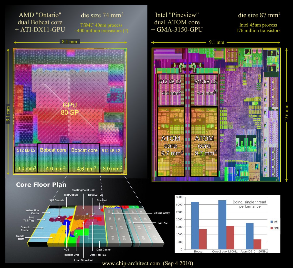
AMD's Ontario
APU will be launched
early 2011 using TSMC's
40nm bulk process. It's
the first incarnation of
AMD's new APU strategy
of combining CPU
and GPU on the
same die.
Striking is how
very small the 40 nm
Bobcat cores are,
especially when compared
those of the 45 nm Atom
cores. At only 4.6 mm2
the Bobcat cores are
less than half the size
of the 9.7 mm2 Atom
cores. It's not only the
core logic, also the
512MB L2 caches of
Ontario are
significantly smaller as
the equal sized Atom
caches: 3.0 mm2 versus
4.4 mm2.
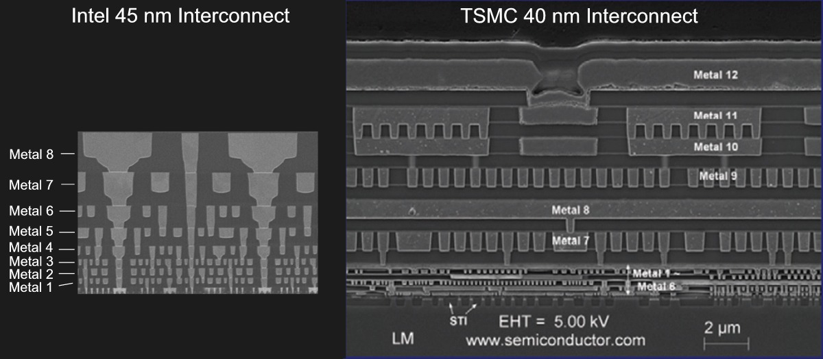
How is this possible?
Have a look at the
detailed
specifications of both
CMOS processes. The TSMC
40nm document is a very
extensive report from
UBM Tech- Insight. It
contains detailed
photographs and
measurements of an FPGA
which is manufactured in
TSMC's 40nm process. The
second one stems from
INTEL's own Technology
Journal.
TSMC's
40 nm process
INTEL's
45 nm process
The most important
process parameters which
determine how dense you
can route your circuits
on silicon are given in
the table at the right.
The contacted
gate pitch
determines the minimum
distance at which you
can put two transistors
together. This is
especially important in
very dense regular
designs like SRAM
arrays. Both Intel and
TSMC claim a minimum
contacted gate pitch
of 160nm. (The UBM
report shows a 167nm
pitch)
More important however
for dense routing is the
metal interconnect which
wires all the
transistors together in
actual circuits. It is
here where TSMC excels.
The first metal layer
(M1), has a wire pitch
of just 120nm, far
smaller as the 160 nm
pitch of Intel's
process.
In fact, the 120nm is
not far from the 112.5
nm metal 1 pitch of
Intel's 32nm process.
This interconnect pitch
is the hardest to
achieve feature of the
entire process. It
requires the most from
the lithography
equipment.
120 versus 160 nm means
that the routing density
is about (160/120)2
= 1.78 times higher for
the TSMC process which
is clearly demonstrated
in the ratio of the CPU
core sizes. For dense
regular designs like
cache memory the
interconnect is less
important. Still the
TSMC cache sram is
~1.45 times denser.
This certainly also
explains why the large
GPU's from ATI and
NVidia can reach such
incredible transistor
densities compared to
the numbers where used
to from the CPU world.
|