March  06, 2003:  Looking at Intel's Prescott die (updated)


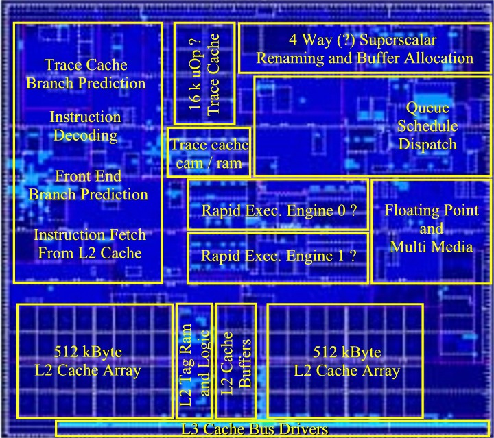
Looking at Intel's Prescott die 

(by Hans de Vries)


 We take a hard look at Intel's Prescott die to sea if we can discover more an undisclosed features


Intel gave it's first presentation on it's new Prescott x86 processor during it's Spring 2003 Developers Forum . 

This processor is to be produced near the end of the year on Intel's new 90 nm strained silicon process. Intel had already stated the Prescott would be a significant extension to the Pentium 4 Netburst architecture and the first glimpses of Prescott layout so just that. It is a completely new lay-out with numerous changes. Looking closely at the die one can see (or at least imagine...) numerous improvements many of them not yet publicly disclosed by Intel. 

  The info given by Intel until now.  


            -   A larger L2 Unified Cache:            1024 kByte versus 512 kByte  for Northwood. 

            -   A larger L1 Data Cache:               16 kByte versus 8 kByte   for Pentium 4 .

            -   An extremely low clock skew:       7 picoseconds versus 22 picoseconds for Northwood.

            -   "La Grande" Support                     protection for providers or consumers?  It's what exactly?   

            -   13 new instructions  (PNI)

Intel states also many improvements.  ( but improved how? )


            -   Improved Hyper threading technology.

            -   Improved pre-fetcher 

            -   Improved branch predictor.

            -   Improved Integer Multiply latency.

            -   Improved Power management.

            -   Additional Write Combining buffers

Our start point:  Intel foils showing (some) layout information:


  In the article below we'll discus the following new features we discovered:


         (1)     Instruction Trace Cache extended from 12 to 16 k uOps ?

         (2)     4 instructions/cycle fetch and retire ? (up from 3)

         (3)     Floating Point unit changed location on the Die

         (4)     Two (!) Rapid Execution Engine's ?

         (5)     Very wide high speed L3 Cache Bus ?

         (6)     Prescott die size 109 mm2 (updated March 7, 2003)


A speculative Die diagram :


The many small white rectangles in the die diagram are so-called Macro-cells. These are block that are pre-routed like Rams and Roms but also critical units that have been laid out by hand such as the high speed ALU's of the Rapid Execution Engine. The automated placement and routing software then handles the rest of die.


  HOME


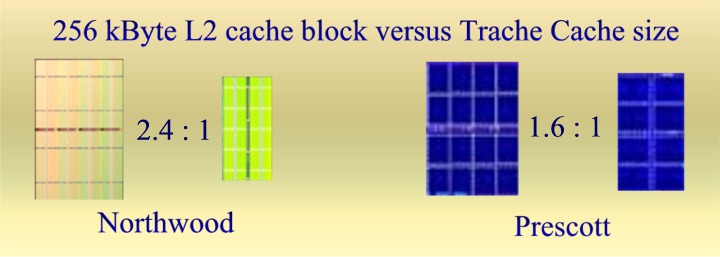
 (1)  Instruction Trace Cache Extended from 12 to 16k uOps ?.


Comparing SRAM sizes 

When we compare the size of the Trace Cache on both Northwood with the size of a 256 kByte L2 Cache block then we see a significant increase.  If we may presume that Intel used it's densest type of SRAM for both large structures then we can obtain an indication of Trace Cache sizes in bytes as well.


                                Northwood Trace Cache:   256 kByte / 2.4   =     ~  106 kByte  +/- ?

                                Prescott Trace Cache:        256 kByte / 1.6   =     ~  160 kByte  +/- ?


 The Trace Cache CPUID

Northwoods Trace Cache contains 12 kOps.  That is 4096 lines of  3 uOps each. One line can be read each cycle. (The actual implementation may provide 6 uOps every 2 cycles, at least according to some patents)

The best place to look for the Prescott Trace Cache size in uOps is the CPUID table. The Trace Cache values were already published with the introduction of the Willamette and are still the same in the latest Prescott PNI document.

 In this table we find the following 3 entries for the Trace Cache. 


70h: 12 kOps,  Trace Cache,  8-way set associative
71h: 16 kOps,  Trace Cache,  8-way set associative
72h: 32 kOps,  Trace Cache,  8-way set associative


So it looks that we might expect a value of 71h in Prescott:   16k uOps.


HOME 


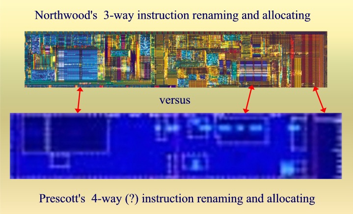
(2)  Four instructions/cycle fetch and retire (up from 3).


Double odd or 4-way

So if we have 16k uOps  (16,384 uOps), how many lines of three uOps do we have?

16,384 / 3 = 5461.33333 lines? or maybe a whole number 5461 then ?  The 3 is already an awkward number. 5461 entries in a memory is something odd as well. It would be possible if the addressing was fully associative but the same CPUID table says that the Trace Cache is 8 way set-associative. What this means is that the number of entries divided by 8 must be a power of 2.  Now clearly 5461/8 = 682.375 is nowhere near a power of 2 !


Doing it four way

We get nice numbers again however if we presume that each Trace Cache entry now has 4 instructions up from 3.

The Trace Cache keeps the same 4096 entries but now with each containing 4 instructions. This would mean that the Prescott can send 4 instructions per cycle into the processing pipeline up from 3.  One can be happy if an average program reaches effectively 1.5  instructions per cycle so 4 per cycle is sufficient to fully support at least 2 threads.


Looking at the layout.

The pipeline stages following the Trace Cache affected by this change would be stages 6 through 9:  ALLOCATE, RENAME1, RENAME2 and QUEUE. These stages are located at the top-right corner of the die. We see that the whole layout has been thoroughly re-arranged, including a total vertical flip. The instructions flow from left to right. At the start we expect micro-code rom plus micro-code sequencer, A queue for incoming instructions from the Trace Cache and the Micro-code sequencer. The Allocate and Rename stages that reserve entries in various buffers further on in the pipeline (outside the area shown above). At the end we expect the Specialized queues for memory access and general integer and floating point instructions. Here ends the 4 way (3 way) division of equal instruction paths.


What goes in must come out:   4 way retiring.

A logical consequence of a 4 instructions per cycle Instruction Trace Cache is the ability to retire the same amount of instructions per cycle. This then at the very end of the pipeline. 


HOME


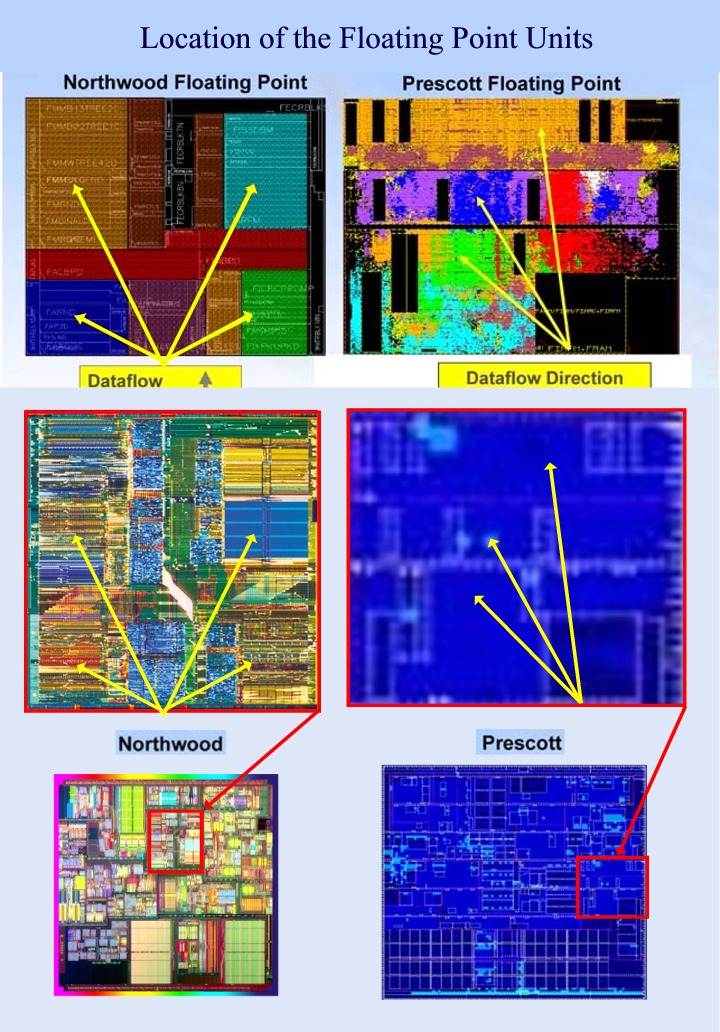
(3)  Floating Point unit changed location on the Die.


Making room for ...

The top two images below are from one of the Intel presentation sheets. They show what the layouter sees on his monitor when looking at the entire Floating Point unit of Northwood and Prescott.  The Prescott view shows how various units are intertwined. This is because the layout software was allowed to place cells anywhere it wanted in the entire area unlike the Northwood view where it was not allowed to place cells outside their bounding box. 


The two middle images show the same Floating Point units. The Northwood version comes from a high resolution die photo while the vague Prescott Floating Point unit was found on Prescott die photo shown during the spring 2003 IDF

The lower two images show the locations have changed. Again this shows that Prescott is a significant change from its Willamette/Northwood predecessors 

HOME

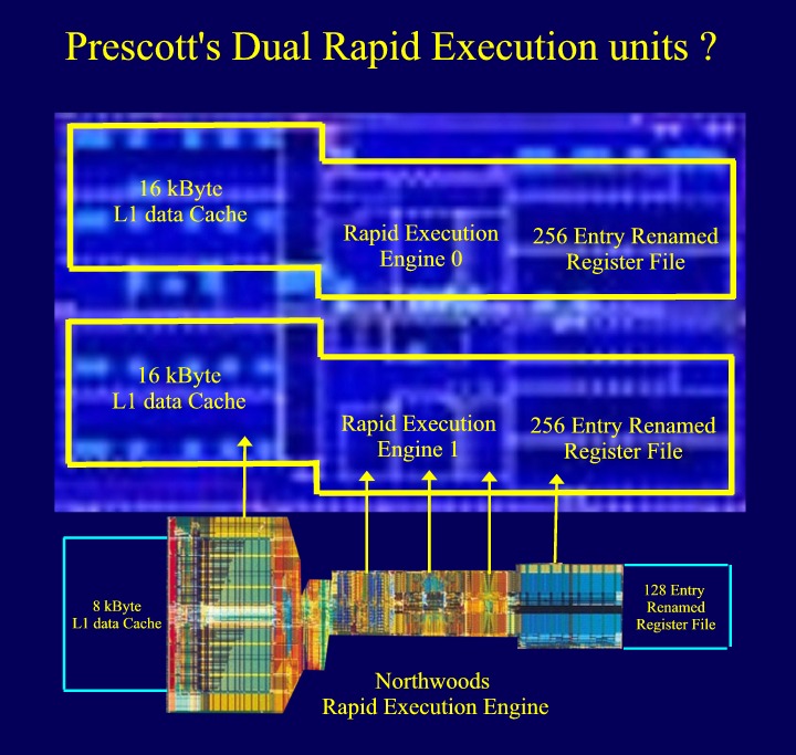
(4)  Two (!) Rapid Execution Engine's ? .


Most remarkable is what we may see at the location where we expect the Rapid Execution Engine and L1 Data Cache.Almost the same location that we know from the Pentium 4. The L1 Data Cache connected to the L2 with its very wide data bus is located close to the middle of the L2 cache. It seems that there are two identical copies, partly mirrored, next to each other. Now when we compared this with the central part of the Northwood's Rapid then we recognize a number of "hand-routed" macro-cells. These macro's are hand-routed because they are the highly speed critical cental units of the Rapid Execution Engine. Units like the ALU's the AGU's and the Bypass network.

Two copies of the L1 Data Cache as well?


It looks like there may be two copies of the L1 data cache as well. Both with the increased size of 16 kByte

HOME 

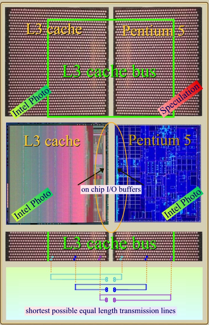
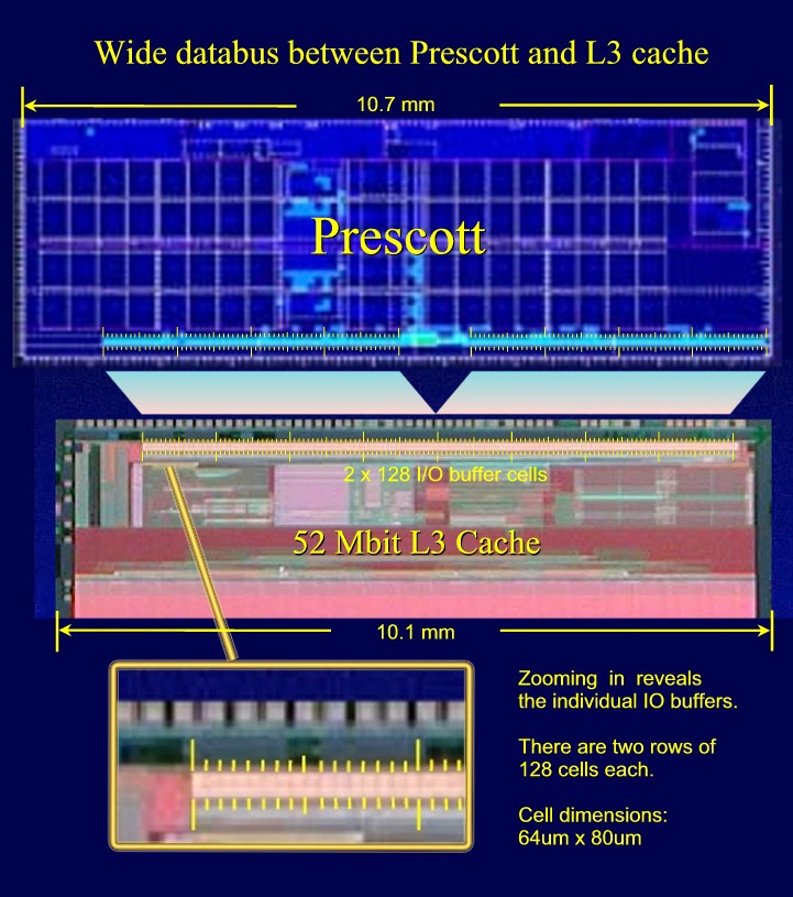
(5)  Very wide high speed L3 Cache Bus ?.

The drawing below stems from a year old article that I never published. The only thing that has changed now is the new die photo of the Prescott. The 52,428,800 bit (presumably) L3 cache sram was the first shown 90 nm device. The L3 cache contains a significant amount of  extra logic and smaller memory that may be Tag Ram.

A lot of IO buffers


One eye catching detail on the L3 cache is the long row of little rectangles that runs along 90% of one of the die-sides.

If we zoom in then we can actually count them: 2 rows of 128 cells. These are most likely IO buffers. The fact that we now see a very similar row at the opposite side on Prescott's makes this only more likely.

Intel did mention that the Sram runs at a frequency higher as the then fastest Pentium 4.  This may mean that the old Xeon tradtion that the L3 cache bus runs at the same frequency as the processor core is continued with the Pentium 5.


One wonders what the relation is with the newly announced 775-contact pinless Land Grid Array (LGA) package with 297 contacts more as the current 478 pin package..


HOME 


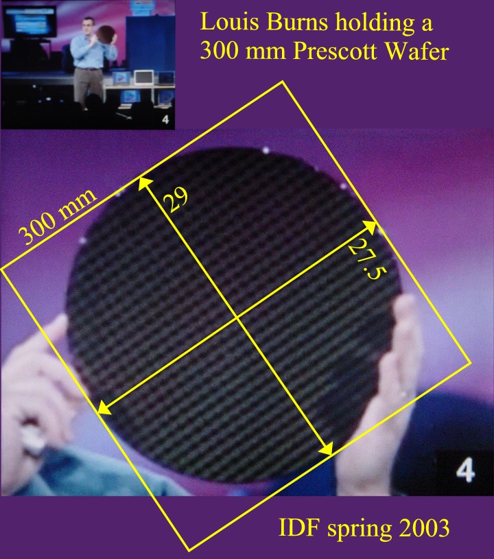
(6)  Prescott die size 109 mm2  (10.7 x 10.2 mm).

(updated March 7, 2003)


 Thanks to Hisa Ando san from Japan:  Prescott's right die size


Thanks to Ando san who wrote how he first calculated Prescott die size from Louis Burns spring 2003 IDF presentation and then found the exact values in presentation 19.7 at the ISSCC 2003: A scalable Sub-10ps Skew Global Clock Distribution for a 90 nm Multi-GHz IA Microprocessor (N. Bindal, T. Kelly, N. Velastegui, R. Raman, K. Wong)

The exact sizes are 10.7 mm x 10.2 mm. The wafer calculations give 10.9 and 10.34 mm from which we must subtract the narrow scribe-lines which are in the order of 100um or so. 


  Pentium 5  Width:    10.7  mm
  Pentium 5  Height:     10.2  mm
  Pentium 5  Die Size:     109  mm2


HOME